
Prof Douglas J. Paul > Strained-Si MOSFETs
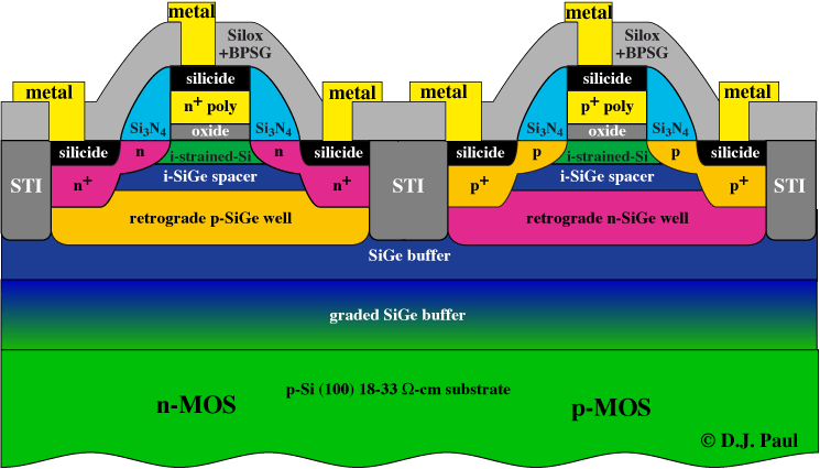
Strained-Si CMOS is on the roadmaps of every major CMOS manufacturer. While working at Cambridge, I developed a number of CMOS processes and strained-Si devices inside the U.K. HMOS Programme. The major reason is that the circuit performance can be substantially increased by increasing the mobility of the electrons and holes in CMOS transistors.
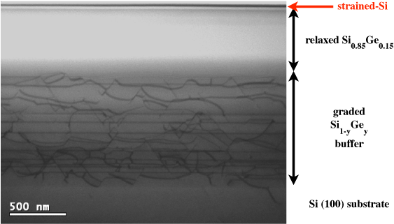
A cross sectional TEM image of a typical virtual substrate with strained-Si cap grown for the U.K. HMOS programme.
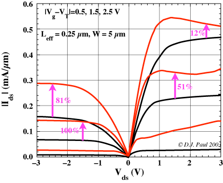
On the right are the IV characteristics from a 0.25 µm CMOS process run as part of the U.K. HMOS programme. The reduction of the current at high voltages is related to self-heating effects as the Si0.8Ge0.2 virtual substrate has a 20 times lower thermal conductivity than Si.
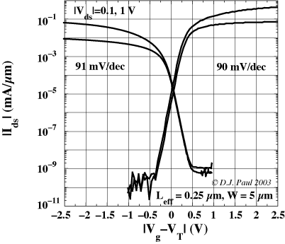
The subthreshold slopes are reasonable for wafers processed in a university cleanroom. As the wafers were processed with a fully thermal budget including a 1050 degree C implant activation for 30 s, Ge diffusion is an issue.