
Prof Douglas J. Paul > Complementary Metal Oxide Semiconductor (CMOS)
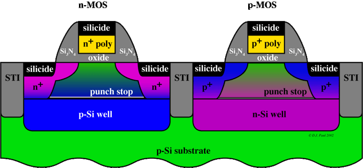
Complementary Metal Oxide Semiconductor (CMOS) circuits require both n- and p-MOSFETs hence the name complementary. The figure above shows a schematic cross-section of typical advanced CMOS devices with low-doped drain contacts implanted through Si3N4 spacers on either side of the gate to reduce the electric field between source and drain. All gates and Ohmic contacts are silicided (using TiSi2, CoSi2 or NiSi) to reduce the resistances of gates and contacts. The reason for CMOS is that the circuit architecture only dissipates power when transistors are switched (i.e. dynamic power dissipation) apart from any leakage currents in the system (i.e. static power dissipation). Below is an animation of a CMOS inverter to demonstrate the principle - press play at the bottom left corner. Current, IDD only flows when the inverter is switched from a 1 to a 0 and so the power consumed is IDD VDD where Vin = Vout = VDD.