Prof Douglas J. Paul > SiGe Strain Relaxation Buffers - SiGe Virtual Substrates
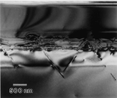
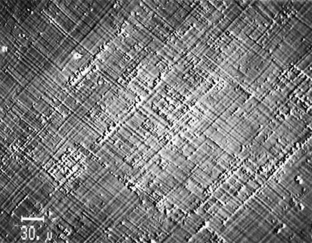
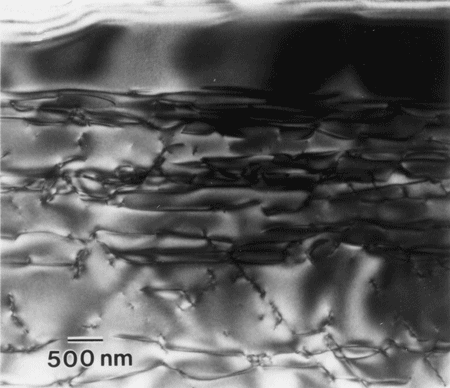
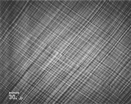
The liquidus solidus curve for Si and Ge results in Si rich phases and Ge rich phases rather than a homogenous mixture of Si1-xGex. There are many types of device where the band structure dictates that a relaxed Si1-xGex layer is required to grow heterolayers on top. The most successful technique to date is to linearly graded the Ge content up to the required Ge content before growing a constant composition buffer on top (see figures below). The highest electronic properties typically result from grading rates below 10% Ge / µm and grown at high temperatures so that the velocity of misfit and threading dislocations is high resulting in a large percentage of misfits travelling completely across the wafer so that the threads fall off the sides of the wafer. As the Ge content is raised the surface roughness is also typically increased.


A cross sectional TEM (on the left) and the surface of the material (on the right) with a grading rate of 24% Ge / µm and final composition of Si0.72Ge0.28. Pictures from wafers grown by D.J. Robbins.


A cross sectional TEM (on the left) and the surface of the material (on the right) with a grading rate of 7% Ge / µm with a final composition of Si0.77Ge0.23. The low temperature mobility of this wafer with a modulation-doped strained-Si quantum well was 361,000 cm2/Vs at 55 mK. Pictures from wafers grown by D.J. Robbins.
