
Prof Douglas J. Paul > Resonant Tunnelling Diodes
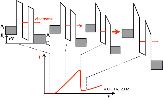
A RTD is basically a quantum well between two tunnel barriers with doped contacts on either side to form reservoirs of electrons (see left).
As a voltage is applied, a current can only flow when electrons can tunnel through the subband state in the quantum well producing a non-linear I-V characteristic useful for certain circuit designs.
 Si/SiGe resonant tunnelling diodes require strained-Si quantum wells on a relaxed virtual substrate typically Si0.8Ge0.2 as shown in the cross sectional TEM image on the left. To prevent the surface segregation effects of AsH3, the wafer was removed from the CVD chamber after the growth of the virtual substrate and the doping of the bottom contact. It was then cleaned using a modified RCA clean before the RTD heterolayers were regrown on top. The thin dark line below the bottom quantum well is contrast at the regrowth interface.
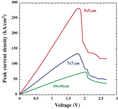
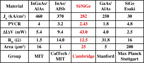
The best results to date at 300 K are shown on the left with a table comparing the results to others in the literature in different technologies. The present RTD results are quite impressive for high frequency circuits.
We are presently working on integrating strained-Si MOSFETs with Si/SiGe RTDs to demonstrate TSRAM circuits.
Significant publications:
- G. Ternent and D.J. Paul, "SPICE modelling of the scaling of resonant tunnelling diodes and the effects of sidewall leakage" IEEE Transactions on Electron Devices 59(12), 3555 (2012) doi 10.1109/TED.2012.2219867
- Z. Suet, D.J. Paul, J. Zhang and S.G. Turner, "Si/SiGe n-type resonant tunneling diodes fabricated using in-situ hydrogen cleaning" Applied Physics Letters 90, 203501 (2007) - doi:10.1063/1.2739089
- G. Ternent and D.J. Paul, "Si/SiGe Tunneling Static Random Access Memories" ECS Transactions 50, pp. 987 - 990 - DOI: 10.1149/05009.0987ecst
- D.J. Paul, P. See, I.V. Zozoulenko, K.-F. Berggren, B. Kabius, B. Holländer and S. Mantl “Si/SiGe electron resonant tunnelling diodes” Applied Physics Letters 77(11), pp1653-1655 (2000) - doi:10.1063/1.1309020
- P. See and D.J. Paul, “Scaled performance of Si/SiGe resonant tunnelling diodes” IEEE Electron Device Letters 22(12), pp 582-584 (2001) - doi:10.1109/55.974584
- P. See, D.J. Paul, B. Holländer, S. Mantl, I.V. Zozoulenko and K.-F. Berggren, “High dc performance Si/Si1-xGex resonant tunelling diodes” IEEE Electron Device Letters 22(4), pp182-184 (2001) - doi:10.1109/55.915607
- D.J. Paul, P. See, I.V. Zozoulenko, K.-F. Berggren, B. Holländer, S. Mantl, N. Griffin, B.P. Coonan, G. Redmond and G.M. Crean “Si/SiGe resonant tunnelling diodes with graded spacer wells” Applied Physics Letters 78(26), pp4184-4186 (2001) - doi:10.1063/1.1381042
- G. Ternent, D.J. Paul, C.N. Ironside, K. Seuranine, D. MacLaren, M.J. Kelly, D. Zuo, D.R. Leadley and M. Myronov, "Sub-50 nm GaAs/AlAs and Si/SiGe Self-Aligned Resonant Tunnelling Diodes (Invited)" UK Semiconductor Conference, Sheffield, July (2011)