
Prof Douglas J. Paul > Quantum Technology
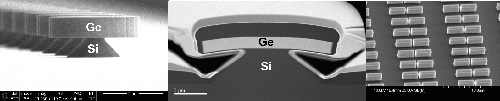
Silicon Nanowire Quantum Dots for Current Standards and Qubits
We have developed an 8 nm diameter silicon nanowire process which has been used to produce sensors, transistors and quantum dots which form the basis of current standards and qubits.
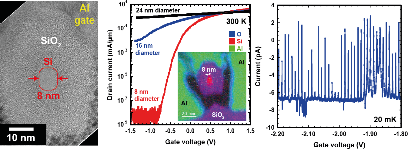
Current standards: We are developing single quantum dot nanowire devices using two wrap around gates which will be a turnstyle to single electrons. By running one of the gates at a frequency f, the current, I through the device is the electron charge, q times the frequency which produces a current standard with I = qf. We are working with NPL and NIST to develop a lot temperature current standard without the need for any magnetic field. By scaling the device down so the quantum dot is of order of 10 nm or less, we are aiming to produce a current standard that could work at room temperature. The vision is to produce single chip current standards that could be integrated into current meters and other scientific or consumer products to allow them to be self-calibrated to the integrated standard.
Qubits: We are working with groups at Oxford, Cambridge and UCL to produce multiple quantum dots with a range of control gates and readout devices to form charge and spin qubits.
- M.M. Mirza, F.J. Schupp, J.A. Mol, D.A. MacLaren, G.A.D. Briggs and D.J. Paul, "One dimensional transport in silicon nanowire junction-less field effect transistors" Scientific Reports 7(1), 3004 (2017) - DOI: 10.1038/s41598-017-03138-5
- C. Busche, L. Vila-Nadal, J. Yan, H.N. Miras, De-L. Long, V.P. Georgiev, A. Asenov, R.H. Pedersen, N. Gadegaard, M.M. Mirza, D.J. Paul, J.M. Poblet and L. Cronin, "Design and fabrication of memory devices based on nanoscale polyoxometalate clusters" Nature 515, Issue 7528, pp. 545 - 549 (2014) - DOI: 10.1038/nature13951
- M.M. Mirza, D.A. MacLaren, A. Samarelli, B.M. Holmes, H. Zhou, S. Thoms, D. MacIntyre and D.J. Paul, "Determining the electronic performance limitations in top-down fabricated Si nanowires with mean widths down to 4 nm" Nano Letters 14(11), pp. 6056 - 6060 (2014) - DOI: 10.1021/nl5015298
- D.J. Paul, J.R.A. Cleaver, H. Ahmed and T.E. Whall “Coulomb blockade in silicon based structures at temperatures up to 50K” Applied Physics Letters 63(5), pp631-632 (1993) - doi:10.1063/1.109972
Germanium on Silicon Single Photon Avalanche Detectors (SPADs)
We have been working with Gerald Buller's group at Heriot-Watt University and we jointly produced the first Geiger mode Ge on Si single photon avalanche detectors (SPADs) at 1310 nm and 1550 nm.
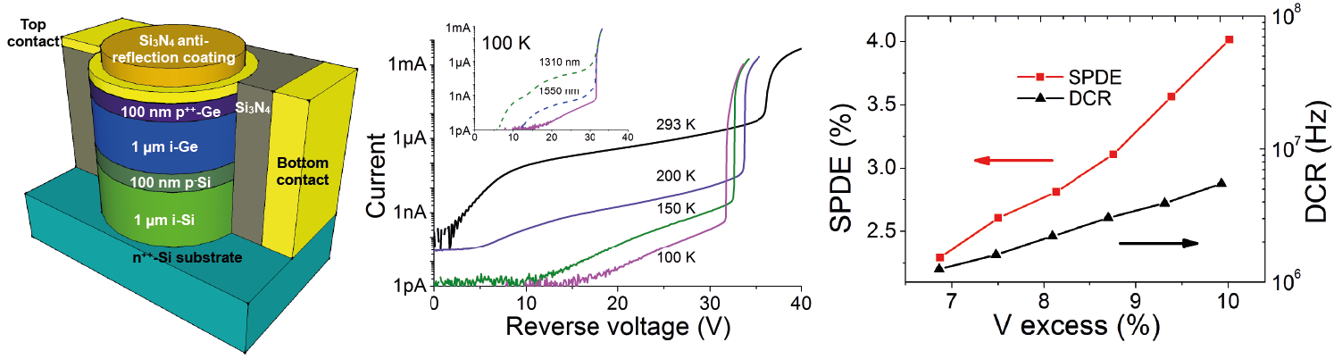
Single photon detectors are key devices for quantum enhanced imaging, quantum optics, quantum communications and a number of photonic based quantum simulation and computing schemes. Commercial InGaAs SPADs are expensive and it is difficult to see them become cheap enough for consumer applications. As part of the QuantiC Quantum Technology Hub, we are therefore developing far cheaper Ge on Si SPADs which could be integrated into Si photonic circuits or build into large imaging arrays. Key markets are for automotive and autonomous vehicle rangefinding, squeezed light imaging and quantum communications.
- R.E. Warburton, G. Intermite, M. Myronov, P. Allred, D.R. Leadley, K. Gallacher, D.J. Paul, N.J. Pilgrim, L.J.M.Lever, Z. Ikonic, R.W. Kelsall, E. Huante-Ceron, A.P. Knights and G.S. Buller "Ge-on-Si Single-Photon Avalanche Diode Detectors: Design, Modeling, Fabrication, and Characterization at Wavelengths 1310 and 1550 nm" IEEE Transactions on Electron Devices 60, pp 3807-3813 (2013) - DOI: 10.1109/TED.2013.2282712
- G. Intermite, R.E. Warburton, M. Myronov, Phil Allred, D.R. Leadley, K. Gallagher, D.J. Paul, N.J. Pilgrim, L.J.M. Lever, Z. Ikonic, R.W. Kelsall, and G.S. Buller, "Design and performance of a prototype mesa-geometry Ge-on-Si single-photon avalanche diode detector at 1310 nm and 1550 nm wavelengths" Proceedings of 2013 IEEE 10th International Conference onGroup IV Photonics (GFP), 2013 pp. 132 - 133 (2013) pp142 - 144 (2013) - DOI: 10.1109/Group4.2013.6644406
Miniature Cold Atom Technology for Atomic Clocks, Quantum Navigators and Magnetometers
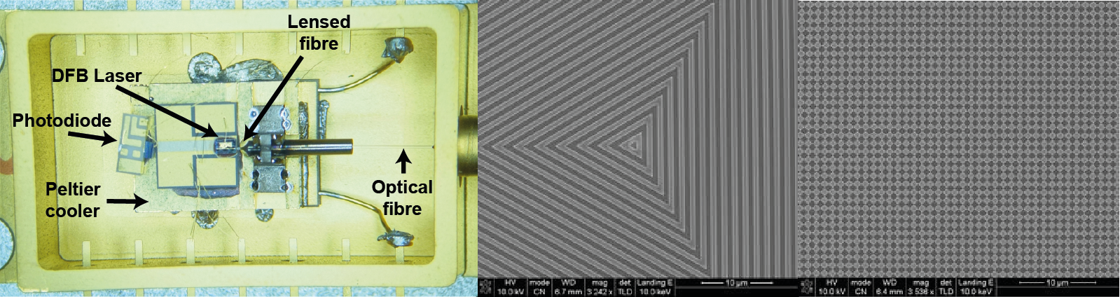
We are part of the UK Quantum Technology Hub for Sensors and Metrology with the aim of developing DFB lasers and miniature components for cold atom systems. The ultimate vision is to develop single chip cold atom systems.
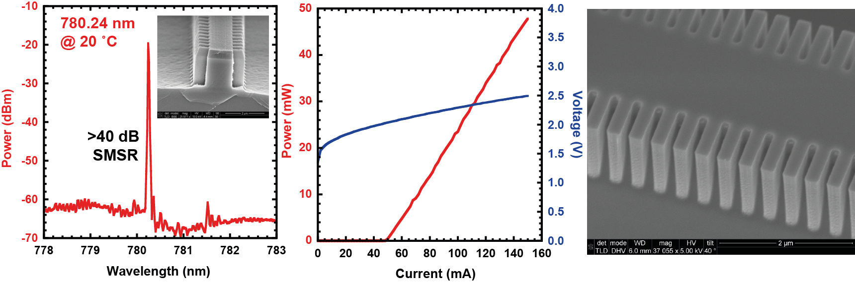
Glasgow has a long history in photonics and lasers and the companies spun out from the University are responsible for manufacturing a significant percentage of the lasers used in telecoms and datacentres globally. We are developing narrow linewidth, fibre-coupled DFB lasers for cold atom systems and in particular Rb. We are also involved in developing integrated locking technology and grating magneto optical traps in miniature vacuum cells with collaborators from the Universities of Strathclyde and Birmingham along with Kelvin Nanotechnology, M Squared Lasers, Optocap and TMD. Below are examples of fibre coupled 780.241 nm DFB lasers operating at 20oC and grating MOTs produced in the James Watt Nanofabrication Centre at Glasgow and published in Nature Nanotechnology 8, 321 (2013): doi: 10.1038/nnano.2013.47.
- K. Bongs et al., "The UK National Quantum Technologies Hub in sensors and metrology (Keynote Paper)" Proceedings SPIE 9900, 990009 (2016) - DOI: 10.1117/12.2232143
MEMS Gravimeter
We have been working with Giles Hammond and colleagues in the Institute for Gravitational Research to develop miniature MEMS gravimeters using the same technology that produces the gyroscope in smart phones.
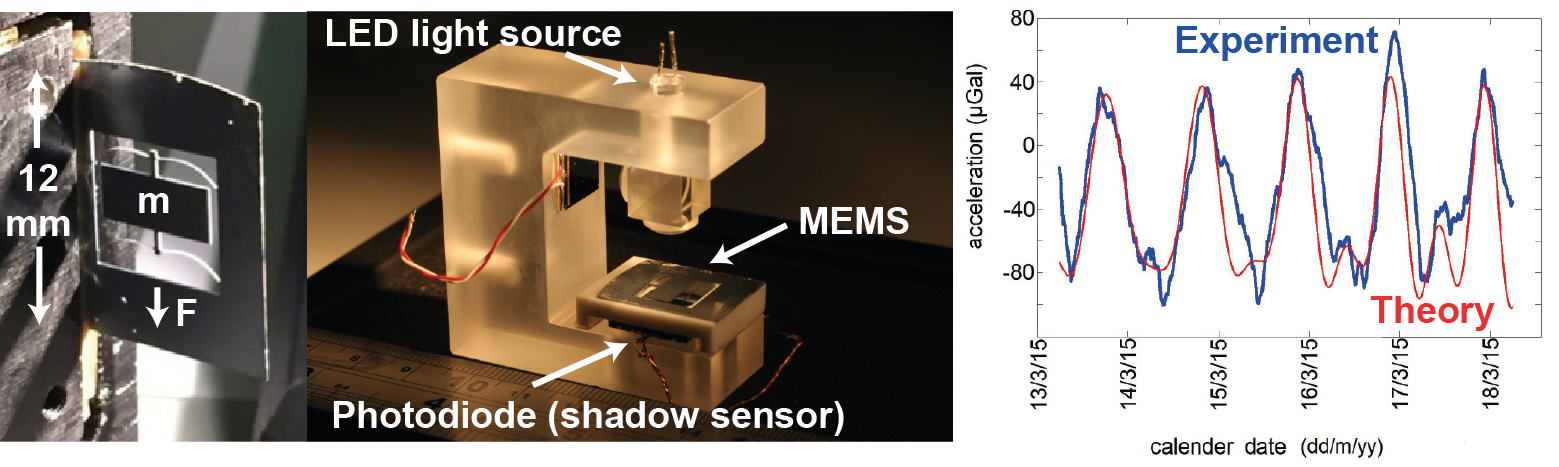
Gravimeters measure the change in gravity using Newton's law of gravity. The device is a mass on a spring using silicon for both. The gravitational force is proportional to the product of the mass of the object being measured and the mass of the gravimeter proof mass divided by the square of the distance between the devices. Such gravimeters are used to characterise geological strata which are used for oil and gas prospecting, detecting sink holes, detecting old mines and for imaging greenfield and brownfield building sites to identify anomalies. We have developed a 12 mm x 12 mm x 0.2 mm MEMS gravimeter chip using anti-springs to reduce the resonant frequency to 1.8 Hz which significantly increases the sensitivity and stability over MEMS accelerometers. Our first MEMS gravimeter achieved 40 µGal/√Hz (about 40 ng/√Hz) which allowed the earth tides to be measured and we are presenting engineering a field portable demonstrator.
- R.P. Middlemiss, A. Samarelli, D.J. Paul, J. Hough, S. Rowan and G. D. Hammond, "Measurement of the Earth tides with a MEMS gravimeter" Nature 531, Issue 7596, pp. 614 - 629 (2016) - DOI: 10.1038/nature17397
- G. Hammond, D.J. Paul and R.P. Middlemiss, "Measurement of acceleration" UK Patent Application No. 1415087, August (2014)
Silicon Quantum Photonics Platform
We are developing a range of components including beam splitters, waveplates, single photon detectors, χ(2) mixers, χ(3) mixers, high-Q microdisk and racetrack cavities and plasmonic antennas to allow integrated silicon quantum photonic circuits to be achieved.
We have already demonstrated the use of strain to engineer the non-linear properties of Ge and We have also used Ge on Si plasmonic antenna to both amplify mid-infrared radiation for chemical sensing and to down-convert and up convert light using the strong χ(3) non-linearity. A range of single photon and broadband mid-infrared detectors are in development which should provide a platform technology for Silicon Quantum Photonics.
- M.P. Fischer, A. Riede, A. Grupp, K. Gallacher, J. Frigerio, G. Pellegrini, M. Ortolani, D. J. Paul, G. Isella, A. Leitenstorfer, P. Biagioni, and D. Brida, "Mid-Infrared Third-Harmonic Emission from Heavily-Doped Germanium Plasmonic Nanoantennas" Conference on Lasers and Electro-Optics, OSA Technical Digest 2017, paper FF1G.2 - DOI: https://doi.org/10.1364/CLEO_QELS.2017.FF1G.2
- M.P. Fischer, C. Schmidt, E. Sakat, J. Stock, A. Samarelli, J. Frigerio, M. Ortolani, D.J. Paul, G. Isella, A. Leitenstorfer, P. Biagioni, and D. Brida, "Optical Activation of Germanium Plasmonic Nanoantennas in the Mid Infrared" Physical Review Letters 117, 047401 (2016) - DOI: 10.1103/PhysRevLett.117.047401
- L. Baldassarre, E. Sakat, J. Frigerio, A. Samarelli, K. Gallacher, E. Calandrini, G. Isella, D.J. Paul, M. Ortolani, P. Biagioni, "Mid-infrared plasmon-enhanced spectroscopy with germanium antennas on silicon substrates" Nano Letters 15(11), pp. 7225 - 7231 (2015) - DOI: 10.1021/acs.nanolett.5b03247
- K. Gallacher, A. Ballabio, R. W. Millar, J. Frigerio, A. Bashir, I. Maclaren, G. Isella, M. Ortolani, and D.J. Paul, "Mid-infrared intersubband absorption from p-Ge quantum wells grown on Si substrates" Applied Physics Letters 108, 091114 (2016) - DOI: 10.1063/1.4943145