
Prof Douglas J. Paul > Nanofabrication
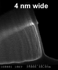
A fundamental part of the research in the group is undertaking developing new nanofabrication process modules that allow new types of devices to be fabricated with high device performance. One example of this research includes the development of sub-4 nm silicon nanowires which have applications for nanowire breath analysis sensors and sensitive electrometers for fundamental science. This involved the integrating separate process modules on sub-5 nm electron beam lithography with HSQ resist, low damage inductively coupled plasma reactive ion etching (ICP-RIE) for process transfer, thermal oxidation for surface passivation and low-resistivity Ohmic contacts. The final devices will be made with lithographic widths between 10 and 20 nm but by fabricating devices at much smaller length scales, the processes can be optimised to maximise the device performance.
It is relatively easy to produce a high aspect ratio vertical silicon nanowire by reactive ion etching if the etch power is increased. The problem with this approach is that the high power results in high energy ions in the plasma which produce a significant amount of process damage to the nanowire and the electrical conductivity will then not be dominated by the nanowire, instead it is dominated by the defect states.
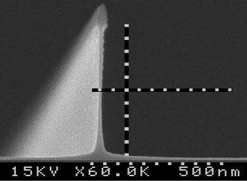
We have developed anisotropic etches using ICP-RIE where the remote plasma allows high density of ions for a high etch rate but then the power for ions etching is reduced to only 4 W. Once the chemistry is optimised, anisotropic silicon nanowires can be fabricated with very low process damage, allowing much higher device performance than devices fabricated by high etch powers. The figure on the right is an example of a high aspect ratio silicon nanowire etched using this technique.
A second example is the development of a low thermal budget Ohmic contact process module to n-type germanium. This has been a difficult problem due to the large Schottky barrier height of most metals and Ge alloy "silicides" on n-type germanium. We undertook work which produced the lowest specific contact resistivity to n-Ge reported at 2.3 ± 1.8 x 10⁻⁷ Ω-cm2.
- M.M. Mirza, P.Velha, G. Ternent, H. P. Zhou, K. E. Docherty and D. J. Paul "Silicon Nanowire Devices with Widths Below 5 nm" Proceedings of the IEEE International Conference on Nanotechnology (Submitted for publication 2012)
- M.M. Mirza, H. Zhou, X. Li, P. Velha, K. Docherty, A. Samarelli, G. Ternent and D.J. Paul, "Nanofabrication of high aspect ratio (~50:1) sub-10 nm silicon nanowires using plasma etch technologies" EIPBN, Hawaii, USA, (May 2012)
- M.M. Mirza, H.P. Zhou, K.E. Docherty, S. Thoms, D.S. MacIntyre and D.J. Paul, "High aspect ratio (~25:1) sub-10 nm HSQ lines using electron beam lithography" EIPBN, Hawaii, USA, (May 2012)
- K. Gallacher, P. Velha, D.J. Paul, I. MacLaren, M. Myranov and D.R. Leadley, "Ohmic contacts to n-type germanium with low specific contact resistivity" Applied Physics Letters 110, 022113 (2012) doi: 10.1063/1.3676667